Novinka:NXP: P89LPC97X - 20-pinové 80C51 s 2/4/8 kB FLASH
(Kategória: Semiconductor-ZONE)
Zaslal EdizonTN
05.05.2010-08:35
Spoločnosť NXP uvoľnila sériu 20-pinových 8-bitových MCU so zrýchleným dvoj-clockovým jadrom 80C51.
Jedná sa o P89LPC970/971/972 zabalených v lacnejších púzdrach, v ktorých nájdete výkonnú architektúru, vykonávajúcu inštrukcie v dvoch až štyroch taktoch, vďaka čomu sú šesť krát rýchlejšie ako štandartné 80C51 mikrokontroléry.
Vlastnosti
Ďaľšie nezanedbateľné vlastnosti
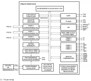
Blokové zapojenie
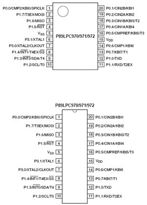
Zapojenie vývodov pre púzdro TSSOP a DIP
Cena
...zatiaľ neurčená. Vzorky sú dostupné.
Odkazy
Homepage
Product Specification
P89LPC970/971/972 User manual
Distribúcia
viď. Adresár
Táto novinka je z mikroZONE
( http://www.mikrozone.sk/news.php?extend.574 )
(Kategória: Semiconductor-ZONE)
Zaslal EdizonTN
05.05.2010-08:35
Spoločnosť NXP uvoľnila sériu 20-pinových 8-bitových MCU so zrýchleným dvoj-clockovým jadrom 80C51.
Jedná sa o P89LPC970/971/972 zabalených v lacnejších púzdrach, v ktorých nájdete výkonnú architektúru, vykonávajúcu inštrukcie v dvoch až štyroch taktoch, vďaka čomu sú šesť krát rýchlejšie ako štandartné 80C51 mikrokontroléry.
Vlastnosti
- 2 kB/4 kB/8 kB byte-erasable flash code memory organized into 1 kB sectors and 64-byte pages. Single-byte erasing allows any byte(s) to be used as non-volatile data storage.
- 256-byte RAM data memory.
- Two analog comparators with selectable inputs and reference source.
- Five 16-bit counter/timers (each may be configured to toggle a port output upon timer overflow or to become a PWM output).
- A 23-bit system timer that can also be used as real-time clock consisting of a 7-bit prescaler and a programmable and readable 16-bit timer.
- Enhanced UART with a fractional baud rate generator, break detect, framing error detection, and automatic address detection; 400 kHz byte-wide I²C- bus communication port.
- SPI communication port (pin remap).
- High-accuracy internal RC oscillator option 7.373 MHz calibrated to ±1 %, with clock doubler option, allows operation without external oscillator components. The RC oscillator option is selectable and fine tunable.
- Watchdog timer with separate on-chip oscillator, nominal 400 kHz/25 kHz, calibrated to ±10 % at 400 kHz, requiring no external components. The watchdog prescaler is selectable from eight values.
- Pin remap for UART, I²C- bus and SPI.
- 2.4 V to 5.5 V VDD operating range.
- Enhanced low voltage (brownout) detect allows a graceful system shutdown when power fails.
- 20-pin TSSOP and DIP packages with 15 I/O pins minimum and up to 18 I/O pins while using on-chip oscillator and reset options. 2 of 66 NXP Semiconductors P89LPC970/971/972 8-bit microcontroller with accelerated two-clock 80C51 core
Ďaľšie nezanedbateľné vlastnosti
- A high performance 80C51 CPU provides instruction cycle times of 111 ns to 222 ns for all instructions except multiply and divide when executing at 18 MHz. This is six times the performance of the standard 80C51 running at the same clock frequency. A lower clock frequency for the same performance results in power savings and reduced EMI.
- Serial flash In-Circuit Programming (ICP) allows simple production coding with commercial EPROM programmers. Flash security bits prevent reading of sensitive application programs.
- Serial flash In-System Programming (ISP) allows coding while the device is mounted in the end application.
- In-Application Programming (IAP) of the flash code memory. This allows changing the code in a running application.
- Clock switching on the fly among internal RC oscillator, watchdog oscillator, external clock source provides optimal support of minimal power active mode with fast switching to maximum performance.
- Idle and two different power-down reduced power modes. Improved wake-up from Power-down mode (a LOW interrupt input starts execution). Typical power-down current is 1 μA (total power-down with voltage comparators disabled).
- Integrated PMU ( Power Management Unit) automatically adjusts internal regulators to minimize power consumption during Idle mode, Power-down mode and total Power-down mode. In addition, the power consumption can be further reduced in Normal or Idle mode through configuring regulators modes according to the applications.
- Active-LOW reset. On-chip power-on reset allows operation without external reset components. A software reset function is also available.
- Configurable on-chip oscillator with frequency range options selected by user programmed flash configuration bits. Oscillator options support frequencies from 20 kHz to the maximum operating frequency of 18 MHz.
- Oscillator fail detect. The watchdog timer has a separate fully on-chip oscillator allowing it to perform an oscillator fail detect function.
- Programmable port output configuration options: quasi-bidirectional, open drain, push-pull, input-only.
- High current sourcing/sinking (20 mA) on eight I/O pins (P0.3 to P0.7, P1.4, P1.6, P1.7). All other port pins have high sinking capability (20 mA). A maximum limit is specified for the entire chip.
- Port ‘input pattern match’ detect. Port 0 may generate an interrupt when the value of the pins match or do not match a programmable pattern.
- Controlled slew rate port outputs to reduce EMI. Outputs have approximately 10 ns minimum ramp times.
- Only power and ground connections are required to operate the P89LPC970/971/972 when internal reset option is selected.
- Four interrupt priority levels.
- Eight keypad interrupt inputs, plus two additional external interrupt inputs.
- Schmitt trigger port inputs.
- Second data pointer.
- Emulation support.
Blokové zapojenie

Zapojenie vývodov pre púzdro TSSOP a DIP
Cena
...zatiaľ neurčená. Vzorky sú dostupné.
Odkazy
Homepage
Product Specification
P89LPC970/971/972 User manual
Distribúcia
viď. Adresár
Táto novinka je z mikroZONE
( http://www.mikrozone.sk/news.php?extend.574 )