Novinka:NXP: Nový Arm® Cortex®-M0+ mikrokontrolér LPC51U68
(Kategória: Semiconductor-ZONE)
Zaslal EdizonTN
03.08.2018-09:21
Toto nové MCU, pinovo kompatibilné s nadupanejšou radou LPC5410x/LPC5411x (ARM Cortex-M4/M0+), dostalo do vienka nielen slušnú pamäť (96 KB SRAM/256 KB Flash), ale aj USB, I2S, SCTimer a 12-bitový 5 Msps AD prevodník, pričom jeho cena sa pohybuje okolo 3.20 Eur.
Čím je tento mikrokontrolér zaujímavý?
V NXP konečne začali harmonizovať pinout mikrokontrolérov*. Táto M0 dostala vylepšené periférie, ktoré boli už použité aj u LPC5410x/LPC5411x. Napríklad UART schopný komunikovať až 6.25 Mbps v asynchrónnom režime a 20 Mbps v synchrónnom (staršie verzie periférie šli iba do 4.5/15 Mbps), ADC schopné ísť až do 5.0 Msps (oproti 2 Msps), I2C zvládajúce až 3.4 Mbps (staršie verzie iba do 1 Mbps), SPI zvládajúce až 71 Mbps oproti 17 Mbps....
Bohužiaľ, ani v tomto mikrokontroléri (ani u LPC5410x/LPC5411x) nenájdeme Switch Matrix - funkcia, umožňujúca prepojiť IO periférie na (skoro) ľubovolný I/O pin púzdra.
Tak isto absentujú analógové komparátory a DA prevodník.
... všetky periférie sú ako cez kopirák s LPC5410x/LPC5411x.
Vlastnosti
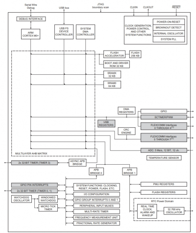
Blokové zapojenie
Cena
Farnell ponúka tieto MCU v cene od 3,10 Eur (kusové množstvá)
Odkazy
*Možno sa nejedná o zámer, možno len pri výrobe LPC54xxx došlo k chybe a M4 jadro sa nerozbehlo, tak preznačili čip a so stávajúcim druhým M0 jadrom je nový produkt na trhu....
Táto novinka je z mikroZONE
( http://www.mikrozone.sk/news.php?extend.1381 )
(Kategória: Semiconductor-ZONE)
Zaslal EdizonTN
03.08.2018-09:21
Toto nové MCU, pinovo kompatibilné s nadupanejšou radou LPC5410x/LPC5411x (ARM Cortex-M4/M0+), dostalo do vienka nielen slušnú pamäť (96 KB SRAM/256 KB Flash), ale aj USB, I2S, SCTimer a 12-bitový 5 Msps AD prevodník, pričom jeho cena sa pohybuje okolo 3.20 Eur.
Čím je tento mikrokontrolér zaujímavý?
V NXP konečne začali harmonizovať pinout mikrokontrolérov*. Táto M0 dostala vylepšené periférie, ktoré boli už použité aj u LPC5410x/LPC5411x. Napríklad UART schopný komunikovať až 6.25 Mbps v asynchrónnom režime a 20 Mbps v synchrónnom (staršie verzie periférie šli iba do 4.5/15 Mbps), ADC schopné ísť až do 5.0 Msps (oproti 2 Msps), I2C zvládajúce až 3.4 Mbps (staršie verzie iba do 1 Mbps), SPI zvládajúce až 71 Mbps oproti 17 Mbps....
Bohužiaľ, ani v tomto mikrokontroléri (ani u LPC5410x/LPC5411x) nenájdeme Switch Matrix - funkcia, umožňujúca prepojiť IO periférie na (skoro) ľubovolný I/O pin púzdra.
Tak isto absentujú analógové komparátory a DA prevodník.
... všetky periférie sú ako cez kopirák s LPC5410x/LPC5411x.
Vlastnosti
- ARM Cortex-M0+ processor, running at a frequency of up to 100 MHz.
- Single cycle multiplier.
- ARM Cortex-M0+ built-in Nested Vectored Interrupt Controller (NVIC).
- Non-maskable Interrupt (NMI) with a selection of sources.
- Serial Wire Debug (SWD) with 4 breakpoints and 2 watchpoints.
- System tick timer.
- On-Chip memory:
- 256 KB on-chip flash programming memory with flash accelerator and 256 Byte page write and erase.
- Up to 96 KB total SRAM composed of up to 64 KB main SRAM, plus an additional 32 KB SRAM.
- 256 KB on-chip flash programming memory with flash accelerator and 256 Byte page write and erase.
- ROM API support:
- Flash In-Application Programming (IAP) and In-System Programming (ISP).
- ROM-based USB drivers (HID, CDC, MSC, DFU). Flash updates via USB.
- Booting from valid user code in flash, USART, SPI, and I2C.
- Legacy, Single, and Dual image boot.
- Flash In-Application Programming (IAP) and In-System Programming (ISP).
- Serial interfaces:
- Eight Flexcomm Interface serial peripherals. Each can be selected by software to be a USART, SPI, or I2C interface. Two Flexcomm Interfaces also include an I2S interface, for a total of 2 channel pairs. Each Flexcomm Interface includes a FIFO that supports USART, SPI, and I2S if supported by that Flexcomm Interface. A variety of clocking options are available to each Flexcomm Interface, and include a shared Fractional Rate Generator.
- I2C supports Fast mode and Fast-mode Plus with data rates of up to 1 Mbit/s and with multiple address recognition and monitor mode. Two sets of true open drain I2C pins also support high-speed Mode (up to 3.4 Mbit/s) as a slave.
- USB 2.0 full-speed host or device controller with on-chip PHY and dedicated DMA controller supporting crystal-less operation in device mode using software library.
- Eight Flexcomm Interface serial peripherals. Each can be selected by software to be a USART, SPI, or I2C interface. Two Flexcomm Interfaces also include an I2S interface, for a total of 2 channel pairs. Each Flexcomm Interface includes a FIFO that supports USART, SPI, and I2S if supported by that Flexcomm Interface. A variety of clocking options are available to each Flexcomm Interface, and include a shared Fractional Rate Generator.
- Digital peripherals:
- DMA controller with 18 channels and 16 programmable triggers, able to access all memories and DMA-capable peripherals.
- Up to 48 General-Purpose I/O (GPIO) pins. Most GPIOs have configurable pull-up/pull-down resistors, open- drain mode, and input inverter.
- GPIO registers are located on AHB for fast access.
- Up to four GPIOs can be selected as pin interrupts (PINT), triggered by rising, falling or both input edges.
- Two GPIO grouped interrupts (GINT) enable an interrupt based on a logical (AND/OR) combination of input states.
- CRC engine.
- DMA controller with 18 channels and 16 programmable triggers, able to access all memories and DMA-capable peripherals.
- Analog peripherals:
- 12-bit ADC with 12 input channels and with multiple internal and external trigger inputs and sample rates of up to 5.0 MS/s. The ADC supports two independent conversion sequences.
- Integrated temperature sensor connected to the ADC
- 12-bit ADC with 12 input channels and with multiple internal and external trigger inputs and sample rates of up to 5.0 MS/s. The ADC supports two independent conversion sequences.
- Timers:
- Three standard general purpose timers/counters, four of which support up to 4 capture inputs and 4 compare outputs, PWM mode, and external count input. Specific timer events can be selected to generate DMA requests.
- One SCTimer/PWM (SCT) 8 input and 8 output functions (including capture and match). Inputs and outputs can be routed to/from external pins and internally to/from selected peripherals. Internally, the SCT supports 10 captures/matches, 10 events and 10 states.
- 32-bit Real-time clock (RTC) with 1 s resolution running in the always-on power domain. A timer in the RTC can be used for wake-up from all low power modes including deep power-down, with 1 ms resolution.
- Multiple-channel multi-rate 24-bit timer (MRT) for repetitive interrupt generation at up to four programmable, fixed rates.
- Windowed Watchdog timer (WWDT).
- Ultra-low power Micro-tick Timer, running from the Watchdog oscillator, that can be used to wake up the device from most low power modes.
- Three standard general purpose timers/counters, four of which support up to 4 capture inputs and 4 compare outputs, PWM mode, and external count input. Specific timer events can be selected to generate DMA requests.
- Clock generation:
- Internal FRO oscillator, factory trimmed for accuracy, that can optionally be used as a system clock as well as other purposes. This oscillator provides a selectable 48 MHz or 96 MHz output, and a 12 MHz output (divided down from the selected higher frequency) that can optionally be used as a system clock as well as other purposes.
- External clock input for up to 25 MHz.
- Watchdog oscillator with a frequency range of 6 kHz to 1.5 MHz.
- 32 kHz low- power RTC oscillator.
- System PLL allows CPU operation up to the maximum CPU rate without the need for a high-frequency external clock. May be run from the internal FRO 12 MHz output, the external clock input CLKIN, or the RTC oscillator.
- Clock output function with divider that can reflect many internal clocks.
- Frequency measurement unit for measuring the frequency of any on-chip or off-chip clock signal.
- Internal FRO oscillator, factory trimmed for accuracy, that can optionally be used as a system clock as well as other purposes. This oscillator provides a selectable 48 MHz or 96 MHz output, and a 12 MHz output (divided down from the selected higher frequency) that can optionally be used as a system clock as well as other purposes.
- Power control:
- Integrated PMU ( Power Management Unit) to minimize power consumption.
- Reduced power modes: sleep mode, deep-sleep mode, and deep power-down mode.
- Wake-up from deep-sleep mode on activity on USART, SPI, and I2C peripherals when operating as slaves.
- Wake-up from sleep, deep-sleep and deep power-down modes from the RTC alarm.
- The Micro-tick Timer can wake-up the device from most reduced power modes by using the watchdog oscillator when no other on-chip resources are running, for ultra-low power wake-up.
- Power-On Reset (POR).
- Brownout detect.
- Integrated PMU ( Power Management Unit) to minimize power consumption.
- JTAG boundary scan supported.
- Unique device serial number for identification.
- Single power supply 1.62 V to 3.6 V.
- Operating temperature range of -40°C to +105°C.
- Available as LQFP64 and LQFP48 packages.
Blokové zapojenie

Cena
Farnell ponúka tieto MCU v cene od 3,10 Eur (kusové množstvá)
Odkazy
*Možno sa nejedná o zámer, možno len pri výrobe LPC54xxx došlo k chybe a M4 jadro sa nerozbehlo, tak preznačili čip a so stávajúcim druhým M0 jadrom je nový produkt na trhu....
Táto novinka je z mikroZONE
( http://www.mikrozone.sk/news.php?extend.1381 )